(Hong Kong)

Product Summary
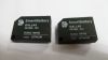
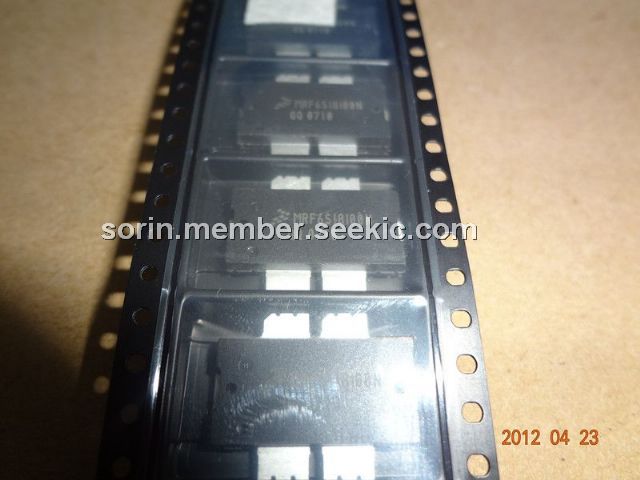
The MRF6S18100N is a RF power field effect transistor.
Parametrics
MRF6S18100N absolute maximum ratings: (1)Drain-source voltage: 68Vdc; (2)gate-source voltage: 12Vdc; (3)total device dissipation: 343W; (4)Storage temperature range: -65 to 175℃; (5)Operating junction temperature: 200℃.
Features
MRF6S18100N features: (1)Characterized with series equivalent large-signal impedance parameters; (2)Internally matched for ease of use; (3)Qualified up to a maimum of 32VDD operation; (4)Integrated ESD protection; (5)Designed for lower memory effects and wide instantaneous bandwidth.
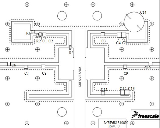
Diagrams
| Image | Part No | Mfg | Description |  |
Pricing (USD) |
Quantity | ||||
|---|---|---|---|---|---|---|---|---|---|---|
 |
 MRF6S18100NBR1 |
Freescale Semiconductor |
Transistors RF MOSFET Power 1990MHZ 28V |
Data Sheet |
Negotiable |
|
||||
|
MRF6S18100NR1 |
Freescale Semiconductor |
Transistors RF MOSFET Power 1990MHZ 28V |
Data Sheet |
Negotiable |
|
||||